Data Fusion using PL, SEM, and EDS Maps
Data Fusion: Integrating and Interpreting Results of Multiple Investigative Measurements
The Klar spectroscopic microscopes provide users with photoluminescence (PL) and Raman spectra, as well as two-dimensional maps, over the deep UV through the near IR range. Emission maps provide a detailed, high-resolution view of the electronic structure of the material, revealing the bandgap and the presence of defects or dislocations due to process damage. Other methods, such as Scanning Electron Microscopy (SEM) or Energy-Dispersive X-ray Spectroscopy (EDS) also reveal information of scientific interest, including structural defects and the presence of specific elements in the sample. When the data from each disparate method is combined, or fused, the investigator can discover the damage or defects, identify its location, and verify via multiple methods how the damage was caused so it may be understood and prevented in future processing. This is essential for the discovery and development of new materials for the semiconductor industry.
A quantitative example is presented below. A gallium oxide sample, annealed in hydrogen, was damaged (as seen by SEM), revealing bright emitters (as seen by PL) that were validated by a Raman spectrum to arise from a Si-CH bond. The presence of silicon (but not gallium) in the bright regions was corroborated using EDS maps. The results and interpretation appear below.

Figure 1. A 355 nm PL map of a gallium oxide sample annealed in hydrogen shows bright 3.27 eV emissions in a few select areas. A subsequent SEM map shows damage in those same areas, as revealed by an overlay of the SEM and PL maps. This suggests the presence of sub-band defects in the damaged regions.

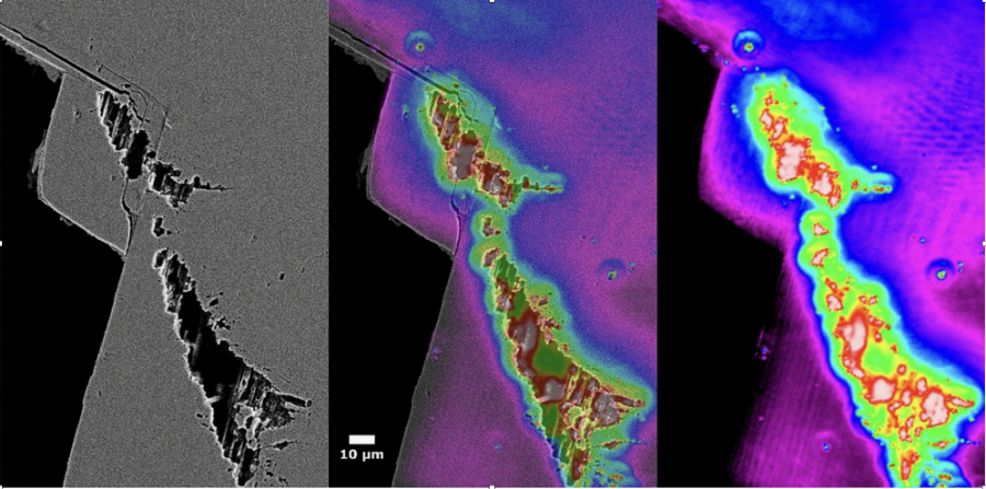
Figure 2. A collage of an SEM, PL map (overlaid onto the SEM), and two EDS maps reveals the presence of strong PL emission from some but not all of the damaged regions of a gallium oxide sample. The EDS maps suggest that the bright PL emissions arise at the same or similar locations as Silicon. The higher concentration of Gallium from some of the damaged areas does not, however, appear to result in any increase of PL.
The presence of silicon in or near the damaged regions may be corroborated using a Raman spectrum, as shown in Figure 3 below.
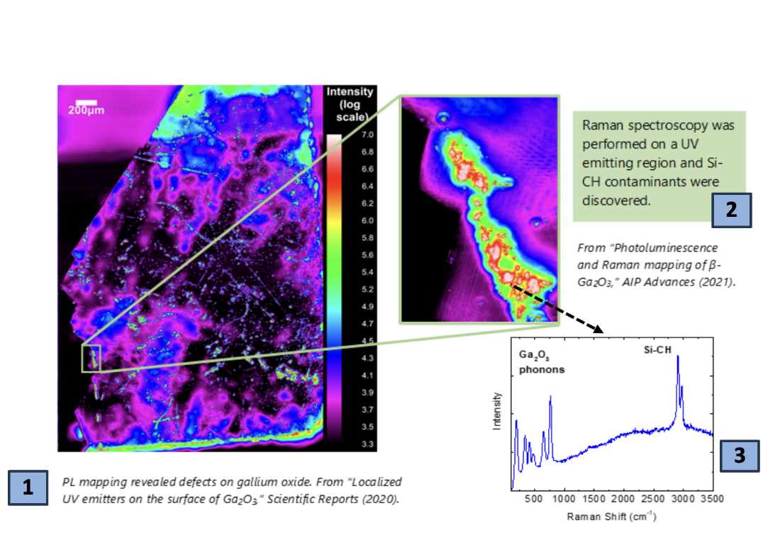
Figure 3 shows how the use of two spectroscopic measurements made by swapping wavelength kits in a Klar instrument capture the bright PL emissions shown in Fig. 1 and reveal the presence of Si-CH bonds at those same locations. This corroborates the EDS fusion collage shown in Fig. 2 and provides the materials scientist with strong evidence of the mechanism and result of damage production in their fabrication process.
From:
Localized UV emitters on the surface of β-Ga2O3, J. Huso, M.D. McCluskey, Y. Yu, Md.M. Islam, and F. Selim, Scientific Reports 10, 21022:1-7 (2020).