
Wafer-Level Scanning
Premium Microscope
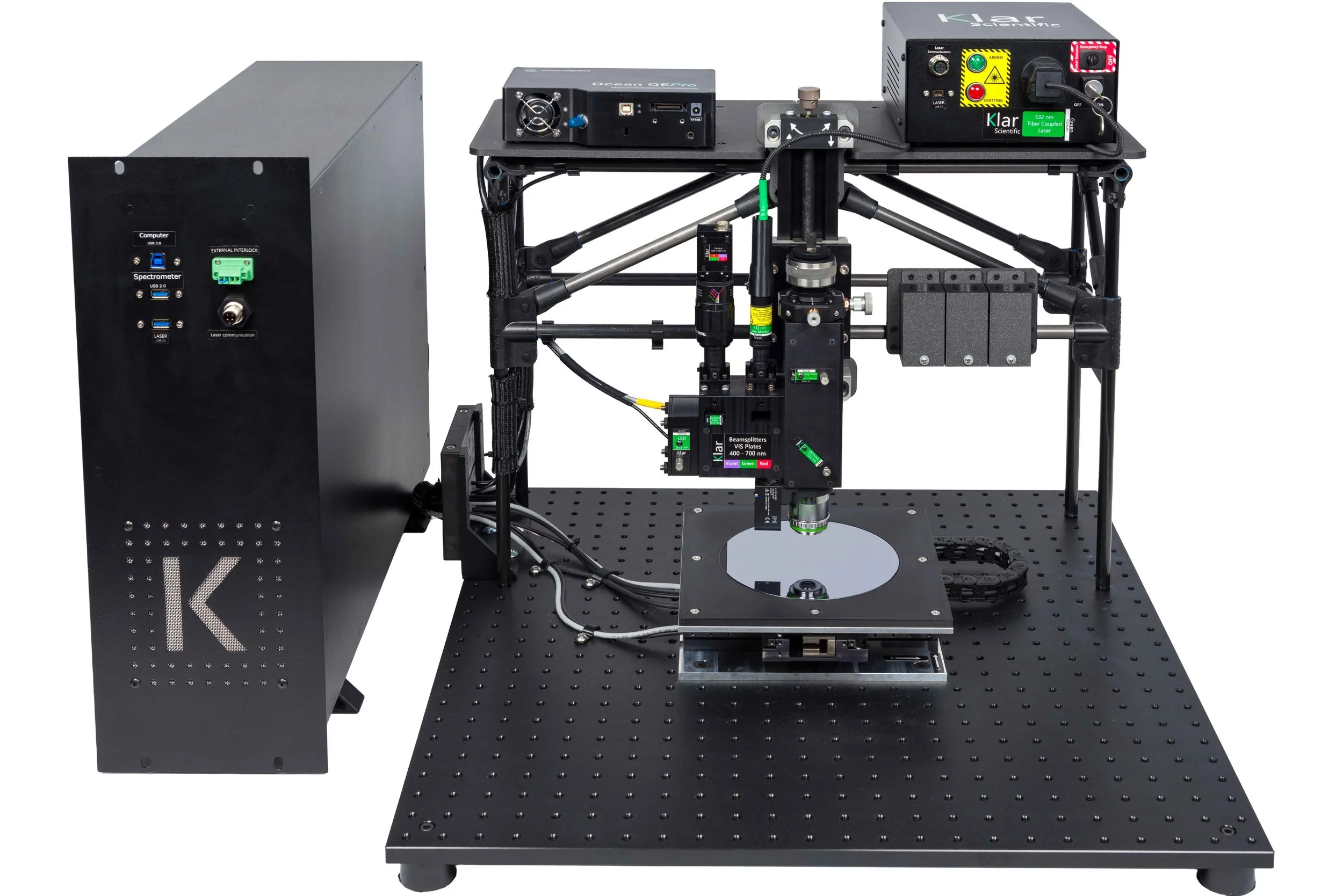
The Klar Premium Microscope has a scanning capacity of 150 mm x 150 mm. It supports probes and other add-ons. Ideal for wafer level studies.
Klar’s Premium microscope system has the same features as the Mini Pro but scans larger areas, 150 mm x 150 mm. These instruments are designed to accommodate additional measurement hardware, including thermal stages, probe tips, pressure cells, and other measurement hardware.
Contact us for a Premium Microscope system quote.
-
Scanning capacity of 150 mm x 150 mm
Supports probes and other add-ons.
Ideal for wafer level studies
Light excitation 349 to 975 nm
COMING SOON
Light excitation 266nmPL spectral range 266 to 2500 nm
Submicron in-plane resolution
Millions of spectra can be collected
GPU accelerated fitting and analysis software
Compact compared to equivalent products
External interlock connector
Integrated laser safety system
Low temperature option
Everything you need to start taking data
Most flexible and versatile microscope
Fits a huge variety of samples
Compatible with the Thorlabs cage rod system
Accommodates many extras
Raman options available
-
The Premium Microscope’s universal optical design allows the owner to expand capabilities with user-replaceable wavelength kits.
Spectroscopy from the near-UV to the near-UV (349 - 1700 nm)
266 nm excitation coming soonChange kits in less than 5 minutes
Custom kits available
-
Scanning capacity of 150 mm x 150 mm. Supports probes and other add-ons, including thermal stages, probe tips, pressure cells, and other measurement hardware.
Customizable Microscope for your Research Lab
Cadmium Telluride
Cadmium telluride (CdTe) and cadmium zinc telluride (CdZnTe, or CZT) are semiconductors with applications in solar cells and particle detection. For the solar cell market, low-cost synthesis techniques must be developed. In semiconductor alloys determination of the concentration of alloy constituents is of considerable importance to understand process dynamics during synthesis. In this example we will use cadmium zinc telluride (CZT) to show how the Zn content of CZT can be mapped using photoluminescence (PL) spectra.
CZT is often grown using the Bridgeman technique in large boules. CZT typically has a weak PL signal and normally displays only a single well-defined peak. Klar’s microscopes are very sensitive, and using our robust modeling of the spectral features, small changes in PL peak energy can be detected.
For this example, a slice of a CZT boule was mapped using a Klar Mini Pro instrument with 532 nm excitation, and the resulting PL spectra were fitted using a single bigaussian function. Figure 1 shows an example spectrum and fit and Figure 2 shows a spatial map of the peak energy. In these fits, available parameters are the emission peak energy, peak amplitude and peak width. We are presently concerned with the peak energy only. Read More….


Fig. 1. Example PL spectrum (black) and fit (red) from a CZT boule. Here a single bigaussian curve is used to model the PL spectrum. Available parameters are peak energy, peak amplitude and peak width.
Fig. 2. False color map of the PL peak energy. Each point shows the value of the peak energy obtained from the spectral fits as shown in Fig. 1
[1] V. Corregidor and E. Dieguez, Correlation of resistivity with zinc content in a vapor grown (Cd,Zn)Te:Se, Appl. Phys. Lett. 81, 5153 (2002); https://doi.org/10.1063/1.1533124