InGaP based optical device
PL
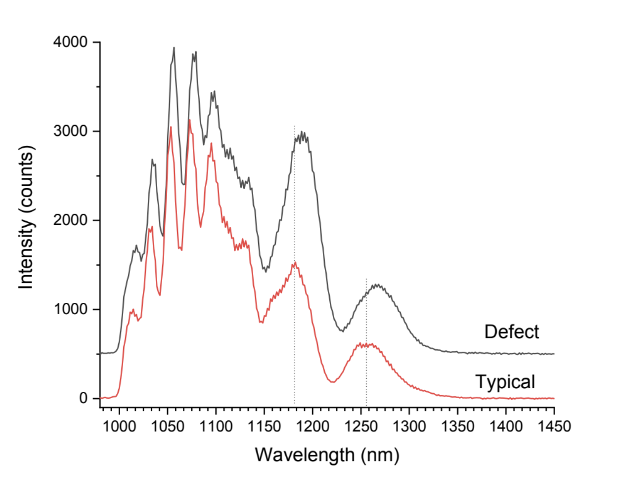
975 nm kit, 10 ms integration time
PL spectra from multiple layers inside the device are readily apparent. This device has embedded defects in the internal layer structure. The spectra of the normal device and a ‘half moon defect’ are noticeably different.
Note that the sharp peaks on the left are due to thin film interference occurring in PL signal confined to a thin layer. The spectra have been offset for clarity.
Sample courtesy of Malcolm Green, Macom